Contents
Getting Started
Downloading and Running ISSIE
Start by clicking the download button on the top-right of your screen. This opens the page of the latest release of ISSIE on GitHub. At the bottom of the page, you can find the latest prebuilt binary for your platform (Windows or Macos). Issie will require in total about 200M of disk space.
- Windows: unzip *.zip anywhere and double-click the top-level
Issie.exeapplication in the unzipped files. - Macos: Double click the dmg file and run the application inside the folder, or drag and drop this to install.
- The binaries are not signed. You will need to perform a one-off security bypass.
Creating a New Project
Once you open Issie you should see two options: New Project and Open Project.
- Click
New Project - Navigate to the folder you want to save your project
- Enter the name of your project
- Click
Create Project
This process creates a folder where your project will be stored and the first sheet of your project, called main. You can see this by clicking at the Sheets selection button.
Your first design
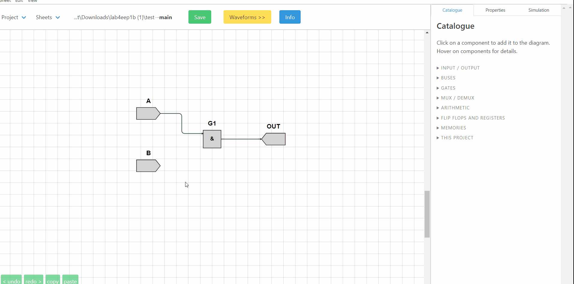
Let’s start with a very simple schematic: a simple 2-input AND gate.
Add the following components to your canvas from the Catalogue tab:
INPUT/OUTPUT=>Input=> Name: ‘A’, Bits: 1INPUT/OUTPUT=>Input=> Name: ‘B’, Bits: 1GATES=>AndINPUT/OUTPUT=>Output=> Name: ‘OUT’, Bits: 1
Now make the appropriate wiring to connect all the components by clicking on one port and dragging the wire to the port you want to connect it to. Connect:
- Input ‘A’ to the first input port of the AND gate
- Input ‘B’ to the second input port of the AND gate
- Output ‘OUT’ to the output port of the AND gate
Your design should look like this:
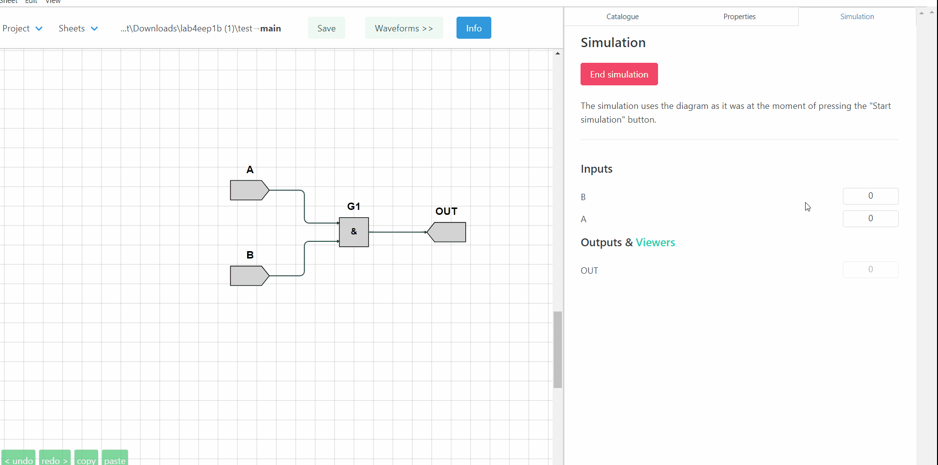
Simulation
Time to simulate our design and see how the output OUT changes as we change the two inputs.
Click the Simulation tab which is located on the top-right corner and then Start Simulation. Now you can change the value of the two inputs and see how the value of the output. Try all 4 combinations of inputs:
- A=0, B=0
- A=0, B=1
- A=1, B=0
- A=1, B=1
and check that the output is correct based on the truth table of the AND gate.
Well Done! You just completed your first ISSIE design.
Exploiting the ISSIE Features
A slightly more complex design
Time to increase the complexity of our design and see how we can exploit the features of ISSIE to create clean and good-looking schematics.
- Add two more inputs named
CandDeach 1-bit. - Add one OR gate and one 2-input MUX
- Delete the output
OUT- Note: You can delete components and/or wires by selecting them and clicking the
deletebutton on your keyboard
- Note: You can delete components and/or wires by selecting them and clicking the
- Add a new 1-bit output
RESULT - Make all necessary connections to achieve a diagram like the one bellow:
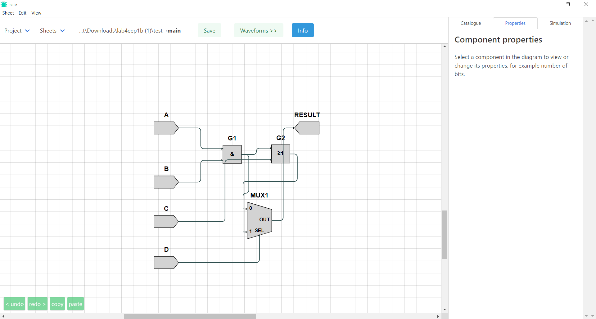
Again, simulate the design and check the output remains correct as you change the values of the 4 inputs
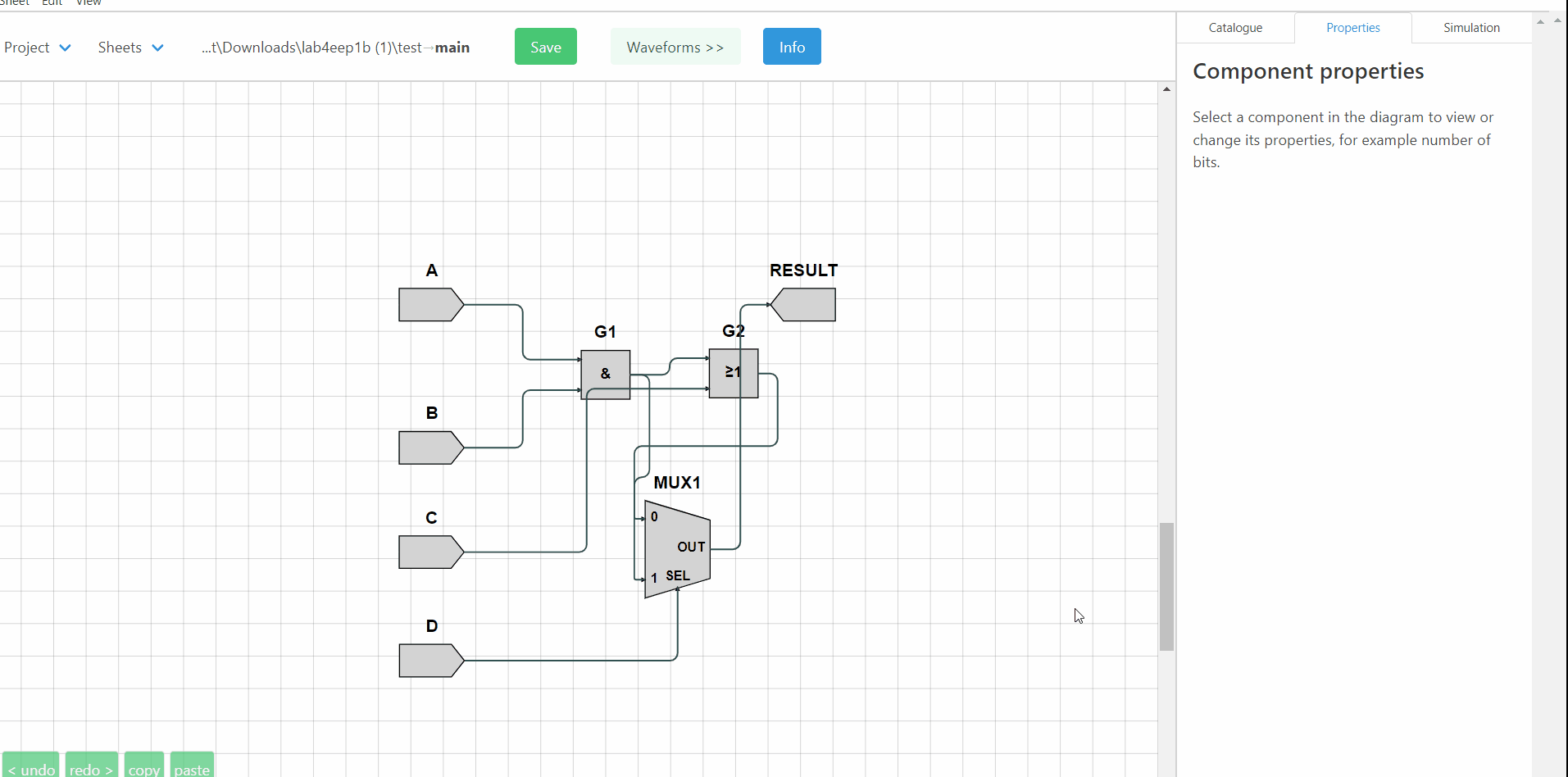
Improving the looking of our design
Clearly, this is a terrible and hard to understand design. Let’s improve it! The ISSIE canvas is fully customisable to allow the creation of readable and good-looking schematics. Specifically, we can:
- Rotate, Flip and Move around all symbols
- Change and Move around the symbols’ labels
- Manually route wires as you like
- Auto-align elements
- Select the wire type we desire (radiussed, jump or modern wires)
You can view the shortcuts for all these modifications by clicking on the edit and view menus.
Let’s now look at our improved schematic:
Summary
- In the
CatalogueMenu we can find an extensive and complete library of components (gates, flip-flops, RAMs, ROMs, n-bit registers) - We can add any number of components in our sheet and name them as we like
- When clicking on a port, ISSIE shows us all the ports we can connect that port to.
- Wires are initially automatically routed
- We can modify our schematic as we like to create a good-looking design.
- We can simulate our design and check how the outputs change as we change the inputs.
Using Custom Components
Your root schematic
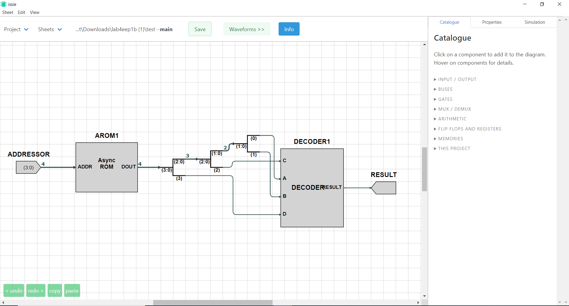
Time now to learn how to use or schematics as cstom components in other design sheets. Here is the idea: The very simple and theoretically useless design we created earlier can be used as a decoder of a 4-bit message to produce a true/false result. Therefore, we are going to create a schematic with an asynchronous-read 4-bit ROM and the schematic we created before as a custom symbol.
Steps:
- Change the name of the current sheet from
maintodecoder(Sheets -> rename) - Add a new sheet and name it
main - Add to the main sheet:
- Asynchronous ROM (
MEMORIES=>ROM (asynchronous)). Select 4 bits addressor, 4 bits data and theEnter data lateroption - Your decoder (
THIS PROJECT=>decoder) - 1-bit output named ‘RESULT’ (
INPUT/OUTPUT=>Output) - 4-bit input named ‘Addressor’ (
INPUT/OUTPUT=>Input)
- Asynchronous ROM (
- Using 3
SplitWirecomponents (BUSES=>SplitWire) separate the 4-bit ROM output to 4 1-bit wires. (see image below) - Make the appropriate connections to achieve the schematic below
Improving the design sheet
It’s time to use another cool feature of Issie: Moving ports in custom components. Issie allows you to re-order and change the side of input and output ports of custom components by CTRL + CLICKING ON THE PORT you want to move.
Let’s look how it works in the gif below:
ROM Initialisation
Currently our ROM is empty as we selected the option Enter Data Later before. Let’s put some values in our ROM.
- Select the ROM and click on the
Propertiestab - Click on
view/edit memory content - Change the content of the 16 memory location available by assigning a random 4-bit number to each one
- Click
done
Simulation
Simulate your design! Change the value of the addressor input and see whether your decoder produces a true or false result for each number you assigned to the ROM.
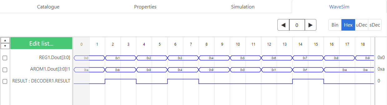
Waveform Simulation
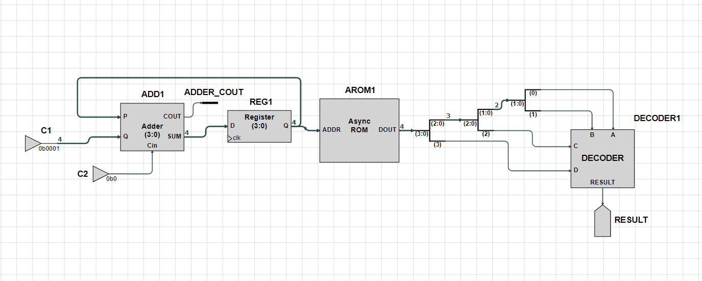
Creating a closed loop design
Let’s now make our top-level design a closed-loop one using a custom addressor which will increment every clock cycle. Now, using the waveform simulator we will be able to view the output of our circuit for all memory locations.
To create an addressor which increments every clock cycle we will need:
- One 4-bit Register (
FLIP FLOPS AND REGISTER=>Register)- NOTE: All clocked components are implicitly connected to the global clock
- One 4-bit Adder (
ARITHMETIC=>N bits adder) - Two Constants (
INPUT/OUTPUT=>Constant):- 0b0001
- 0b0
- Two wire labels (
INPUT/OUTPUT=>Wire Label)- One for
Coutof adder - One for
result - NOTE: Labels are necessary to prevent an unused output from giving an error
- One for
Create a schematic like the one below:
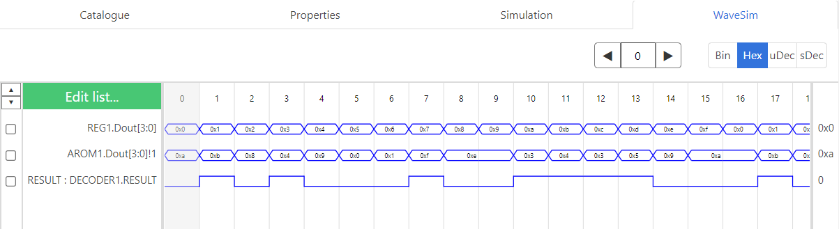
Simulating your design
As soon as you connect everything correctly you should see the Waveforms >> button changing to green. You can now simulate your design.
- Click the
Waveforms >>button - Select:
AROM1.Dout[3:0]REG1.Dout[3:0]RESULT: DECODER1.RESULT
- Click
View - Change the data to either
hexorbinto make them more readable - Check that the waveform simulator output matches your previous (Step Simulation) results
Changing your design
!!! IMPORTANT NOTE: Before you do anything else, you MUST close the waveform simulator.
This is done by clicking Edit list... and then Close !!!
Now add an extra register between your adder and the ROM address (or make any other change you want) and check that the simulation has the expected output.
Now what?
You now know how to use ISSIE to create & simulate digital designs.
You can now create your designs (from simple circuits to fully functionable CPUs) and either simulate them or extract them as Verilog to use them with other tools.